A Leader in Light
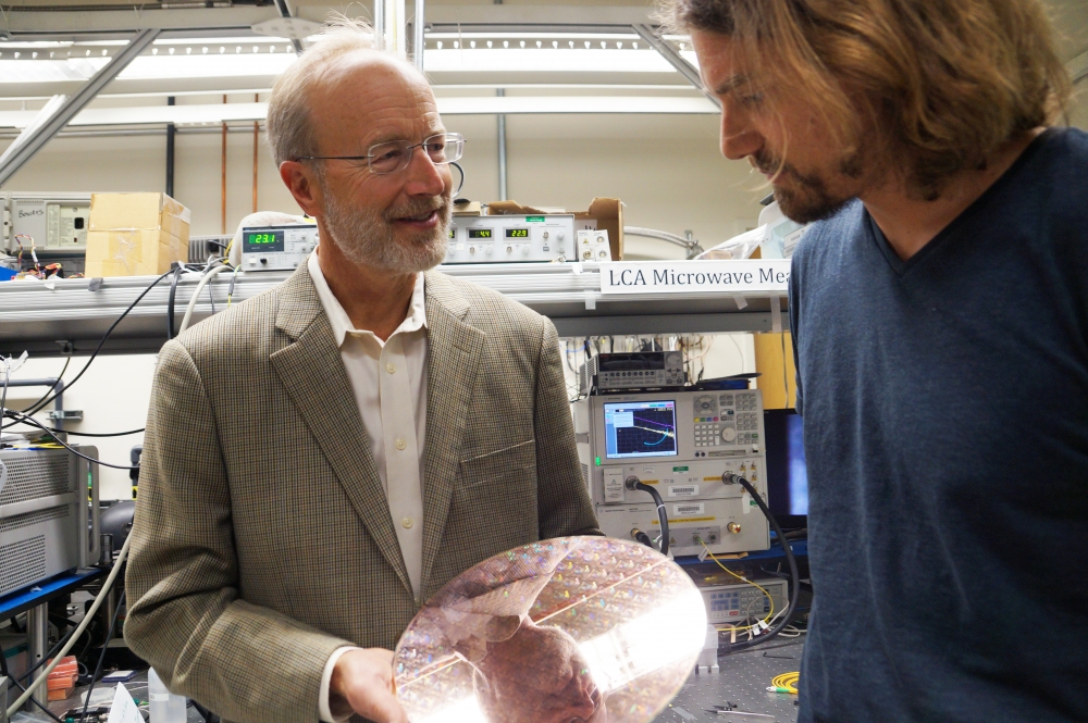
John Bowers, a professor of electrical and computer engineering and of materials at UC Santa Barbara, has been selected to receive the 2017 Institute of Electrical and Electronics Engineers (IEEE) Photonics Award. Bowers is the first faculty member from UCSB to receive the honor, which recognizes his “pioneering research in silicon photonics, including hybrid silicon lasers, photonic integrated circuits and ultra low-loss waveguides.”
“Silicon photonics has the potential to revolutionize photonics and electronics by enabling low-cost, high-volume manufacturing of optical interconnects with a path toward embedding high-capacity fiber optics on circuit boards and eventually on electronic chips,” said Bowers, who holds the Fred Kavli Chair in Nanotechnology at UCSB and is director of the campus’s Institute for Energy Efficiency. An internationally renowned authority on optoelectronics, Bowers has focused his expertise on silicon photonics and optoelectronics, with the goals of developing energy-efficient technology for the next generation of optical networks.
“This is a major award,” said Rod Alferness, dean of the UCSB College of Engineering, who received an IEEE Photonics Award in 2005, before coming to UCSB. “The IEEE Photonics Award is the most prestigious recognition of contributions to the field of photonics and optics. John Bowers’ work in integrated silicon photonics is leading the way to the future of electronics and telecommunications.”
As the demand for bandwidth increases — thanks to the proliferation of computers, mobile devices, smart technology and apps — so will the strain on existing communications infrastructure. Steps have been taken over the last couple of decades to provide the kind of speed, capacity and processing necessary to manage the tidal wave of data generated every day in the form of optic and photonic technology — the use of light to transmit information.
But with new technology comes greater demand. Mobile devices are on the rise, along with data-intensive apps, as well as the Internet of Things — a network of smart objects that communicate not only with their users, but also with each other. To satisfy both capacity and performance requirements, experts say, optics and photonics must be more deeply integrated into our electronics and telecommunications systems.
But here’s the rub: Fiber optics uses photons to transmit data over long distances (and to and from data centers) while computers use electrons to communicate. And the two don’t match. In addition, fiber optics uses indium phosphide wafers and foundries, which is incompatible with electronics’ silicon wafers and foundries.
The answer lies in integrating optics and electronics on the same chip so the electrical signal is converted into an optical one without equalization. It’s a process Bowers has been investigating heavily in his research and also as director for the West Coast center for AIM Photonics, a federally funded manufacturing consortium established to boost photonics manufacturing and create more skilled, high-tech jobs to the country.
Bowers, who came to UCSB in 1987, is a member of the National Academy of Engineering and the National Academy of Inventors, a fellow of the IEEE, Optical Society of America (OSA) and the American Physical Society. He is a recipient of the OSA Holonyak Prize, and the IEEE LEOS William Streifer Award. He and colleagues received the 2007 Annual Creativity in Electronics Award for Most Promising Technology for the hybrid silicon laser.
Share this article
Related Stories


