Ultrasensitive Biosensor from Molybdenite Semiconductor Outshines Graphene
Move over, graphene. An atomically thin, two-dimensional, ultrasensitive semiconductor material for biosensing developed by researchers at UC Santa Barbara promises to push the boundaries of biosensing technology in many fields, from health care to environmental protection to forensic industries.
Based on molybdenum disulfide or molybdenite (MoS2), the biosensor material — used commonly as a dry lubricant — surpasses graphene’s already high sensitivity, offers better scalability and lends itself to high-volume manufacturing. Results of the researchers’ study have been published in ACS Nano.
“This invention has established the foundation for a new generation of ultrasensitive and low-cost biosensors that can eventually allow single-molecule detection — the holy grail of diagnostics and bioengineering research,” said Samir Mitragotri, co-author and professor of chemical engineering and director of the Center for Bioengineering at UCSB. “Detection and diagnostics are a key area of bioengineering research at UCSB and this study represents an excellent example of UCSB’s multifaceted competencies in this exciting field.”
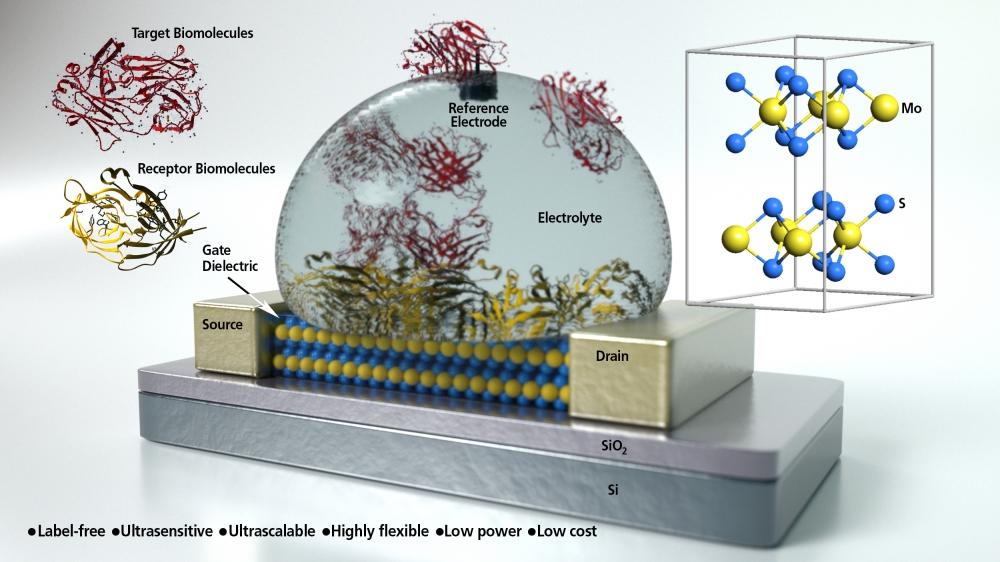
The key, according to UCSB professor of electrical and computer engineering Kaustav Banerjee, who led this research, is MoS2’s band gap, the characteristic of a material that determines its electrical conductivity.
Semiconductor materials have a small but nonzero band gap and can be switched between conductive and insulated states controllably. The larger the band gap, the better its ability to switch states and to insulate leakage current in an insulated state. MoS2’s wide band gap allows current to travel but also prevents leakage and results in more sensitive and accurate readings.
The limitations of graphene
While graphene has attracted wide interest as a biosensor due to its two-dimensional nature that allows excellent electrostatic control of the transistor channel by the gate, and high surface-to-volume ratio, the sensitivity of a graphene field-effect transistor (FET) biosensor is fundamentally restricted by the zero band gap of graphene that results in increased leakage current, leading to reduced sensitivity, explained Banerjee, who is also the director of the Nanoelectronics Research Lab at UCSB.
Graphene has been used, among other things, to design FETs — devices that regulate the flow of electrons through a channel via a vertical electric field directed into the channel by a terminal called a “gate.” In digital electronics, these transistors control the flow of electricity throughout an integrated circuit and allow for amplification and switching.
In the realm of biosensing, the physical gate is removed, and the current in the channel is modulated by the binding between embedded receptor molecules and the charged target biomolecules to which they are exposed. Graphene has received wide interest in the biosensing field and has been used to line the channel and act as a sensing element whose surface potential (or conductivity) can be modulated by the interaction (known as conjugation) between the receptor and target molecules that results in net accumulation of charges over the gate region.
However, said the research team, despite graphene’s excellent characteristics, its performance is limited by its zero band gap. Electrons travel freely across a graphene FET — hence, it cannot be “switched off” — which in this case results in current leakages and higher potential for inaccuracies.
Much research in the graphene community has been devoted to compensating for this deficiency, either by patterning graphene to make nanoribbons or by introducing defects in the graphene layer — or using bilayer graphene stacked in a certain pattern that allows band gap opening upon application of a vertical electric field — for better control and detection of current.
Enter MoS2, a material already making waves in the semiconductor world for the similarities it shares with graphene, including its atomically thin hexagonal structure, and planar nature, as well as what it can do that graphene can’t: act like a semiconductor.
“Monolayer or few-layer MoS2 have a key advantage over graphene for designing an FET biosensor: They have a relatively large and uniform band gap (1.2-1.8 eV, depending on the number of layers) that significantly reduces the leakage current and increases the abruptness of the turn-on behavior of the FETs, thereby increasing the sensitivity of the biosensor,” said Banerjee.
‘The best of everything’
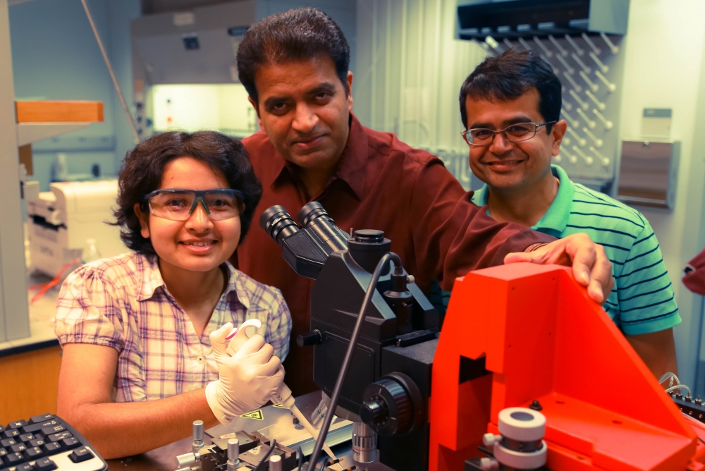
Additionally, according to Deblina Sarkar, a PhD student in Banerjee’s lab and the lead author of the article, two-dimensional MoS2 is relatively simple to manufacture.
“While one-dimensional materials such as carbon nanotubes and nanowires also allow excellent electrostatics and at the same time possess band gap, they are not suitable for low-cost mass production due to their process complexities,” she said. “Moreover, the channel length of MoS2 FET biosensor can be scaled down to the dimensions similar to those of small biomolecules such as DNA or small proteins, still maintaining good electrostatics, which can lead to high sensitivity even for detection of single quanta of these biomolecular species,” she added.
“In fact, atomically thin MoS2 provides the best of everything: great electrostatics due to their ultra-thin body, scalability (due to large band gap), as well as patternability due to their planar nature that is essential for high-volume manufacturing,” said Banerjee.
The MoS2 biosensors demonstrated by the UCSB team have already provided ultrasensitive and specific protein sensing with a sensitivity of 196 even at 100 femtomolar (a billionth of a millionth of a mole) concentrations. This protein concentration is similar to one drop of milk dissolved in a hundred tons of water. An MoS2-based pH sensor achieving sensitivity as high as 713 for a pH change by one unit along with efficient operation over a wide pH range (3-9) is also demonstrated in the same work.
“This transformative technology enables highly specific, low-power, high-throughput physiological sensing that can be multiplexed to detect a number of significant, disease-specific factors in real time,” commented Scott Hammond, executive director of UCSB’s Translational Medicine Research Laboratories.
Biosensors based on conventional FETs have been gaining momentum as a viable technology for the medical, forensic and security industries since they are cost-effective compared to optical detection procedures. Such biosensors allow for scalability and label-free detection of biomolecules — removing the step and expense of labeling target molecules with florescent dye. “In essence,” continued Hammond, “the promise of true evidence-based, personalized medicine is finally becoming reality.”
“This demonstration is quite remarkable,” said Andras Kis, professor at École Polytechnique Fédérale de Lausanne in Switzerland and a leading scientist in the field of 2D materials and devices. “At present, the scientific community worldwide is actively seeking practical applications of 2D semiconductor materials such as MoS2 nanosheets. Professor Banerjee and his team have identified a breakthrough application of these nanomaterials and provided new impetus for the development of low-power and low-cost ultrasensitive biosensors,” continued Kis, who is not connected to the project.
Wei Liu and Xuejun Xie from UCSB’s Department of Electrical and Computer Engineering and Aaron Anselmo from the Department of Chemical Engineering also conducted research for this study. Research on this project was supported by the National Science Foundation, the California NanoSystems Institute at UCSB and the Materials Research Laboratory at UCSB, a National Science Foundation MRSEC.
Share this article
Related Stories


