The Cadence of Electronics Innovation
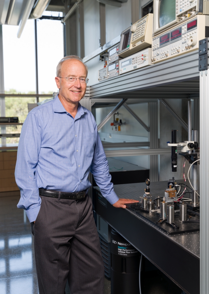
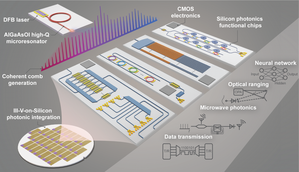
UC Santa Barbara professor John Bowers, the Fred Kavli Chair in Nanotechnology, for several years has worked on a project within the Defense Advanced Research Projects Agency Direct On-Chip Digital Optical Synthesizer (DODOS) program. Together with the teams of Kerry Valhala at Caltech and Tobias Kippenberg at the Swiss Federal Institute of Technology, he developed the first commercially scalable integrated on-chip semiconductor laser and resonator capable of producing a laser microcomb.
Created by the coupled laser and resonator, a microcomb is a series of equally spaced, low-noise, highly stable laser lines, each able to carry data, that dramatically increases the capacity and efficiency of large integrated circuits. The researchers described their achievement in the 2021 paper “Laser soliton microcombs heterogeneously integrated on silicon,” published in Science.
Now, nearly a year later, an article in Nature describes what Bowers, also director of UCSB’s Institute for Energy Efficiency, called a “validation” of the integrated laser-resonator technology detailed in the previous study. “This paper is about bridging the integrated comb technology we developed earlier and PIC [photonic integrated circuit] technology for transmitting and receiving very-high-capacity data streams,” he says.
The authors, led by Prof. Xingjun Wang at Peking University in Beijing, plus Bowers and researchers in his lab, describe what they call “the first integrated chip-scale microcomb-based photonic data link.” Bowers sees it as an important step in reaching the next milestone in the convergence of photonics and electronics.
For some time now, Bowers explained, long-distance data transmission over the internet has been achieved via fiber optics, which makes it possible to move very large amounts of data over long distances with very low loss and using very little power. Previously, the interface between photonics and electronics has been at the edge of a circuit board, but now, says Bowers, “It is inside the package.” This is because electronic chips are growing rapidly in terms of the amount of data being sent to and from them. Current state-of-the-art chips have input-output capacity of up to 51 terabits per second (Tbps), which is 5,000 times the 10 Gbps capacity of a modern desktop computer.
“You have 5,000 times the amount of data going off an advanced switching chip as you have coming out of your computer processor,” said Lin Chang, a researcher in Bowers’ group. “The only way to move that much data is to do it optically, so optics are now inside that switch package.”
Moving so much data, he adds, requires either many lasers, which is not practical given that lasers are comparatively large and must be tightly controlled, or a different technology. Laser-comb technology allows a single laser to drive hundreds of wavelengths via a microcomb, with each wavelength able to carry data. “That’s where the world is going,” Chang says.
That continued expansion of integrated-circuit complexity and capability is not stopping. And it is, essentially, codified within the global electronics industry, helping companies to budget time and resources to arrive at established milestones on time.
“It’s a straight line [of development] and everybody plans for that. That’s their cadence,” Bowers explains. “The switch industry was at 3.2, then 6.4, 12.5, and 25.6 Tbps. Now, we’re at 51 Tbps, and in two years, we’ll be at 102 Tbps. So, you will have to have twice the capacity in just two years and four times as much in four years. That’s why the scalability of the laser-resonator technology is so important.”
As chip performance has steadily increased, the transistor count on a chip, Bowers notes, has gone from about one thousand in 1970, to one hundred million in 2000, to ten billion now — an evolution made possible by the continuous miniaturization of the transistors themselves, the smallest of which are now 5 nanometers (nm) across.
“In moving from 45 nm to 5 nm, however, electronics didn’t get significantly faster. That’s why you need to go more in parallel,” he says, referring to the dramatically capacity-expanding laser-comb technology. “The laser-comb technology provides a promising way for industry to adhere to its cadence, and the data-link system described in the Nature paper demonstrates that promise is being delivered.”
Share this article
Related Stories


