
Full(erene) Potential
In what could be called a classic “Eureka” moment, UC Santa Barbara materials researchers have discovered a simple yet effective method for mastering the electrical properties of polymer semiconductors. The elegant technique allows for the efficient design and manufacture of organic circuitry (the type found in flexible displays and solar cells, for instance) of varying complexity while using the same semiconductor material throughout.
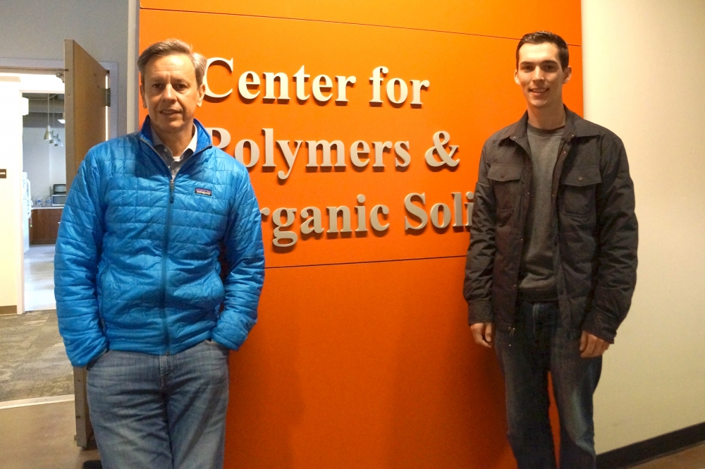
“It’s a different strategy by which you can take a material and change its properties,” said Guillermo Bazan, a professor of chemistry and materials at UCSB. With the addition of fullerene or copper tetrabenzoporphyrin (CuBP) molecules in strategic places, the charge carriers in semiconducting materials — negative electrons and positive “holes” — may be controlled and inverted for better device performance as well as economical manufacture. The discovery is published in a pair of papers that appear in the journals Advanced Functional Materials and Advanced Electronic Materials.
In the realm of polymer semiconductors, device functionality depends on the movement of the appropriate charge carriers across the material. There have been many advances in the synthesis of high-mobility, high-performance materials, said lead author Michael Ford, graduate student in materials, but the fine control of the electrons and holes is what will allow these sophisticated polymers to reach their full potential.
“There’s been a large effort to make new materials, but a lot of them may not be appropriate in conventional low-power devices,” said Ford. Many of these materials exhibit “ambipolar” conduction, meaning that they transport both negative and positive charges, he explained. So, in situations where only a certain charge is required, the opposite charge is also conducting, which diminishes the utility of the material.
“They’re always ‘on’ so you always have a current running through the device,” Ford said. Conventional means of controlling the movement of charge carriers often involves more complex measures, such as multiple metal evaporation steps or depositing additional layers that are difficult to manage. These actions often require more complicated processing or fabrication, which could in the end defeat the purpose of low-cost flexible electronics.
This new development was actually a classic accidental scientific discovery, according to Ford, who was investigating, simultaneously, the properties of two materials. He observed that the use of fullerene additives limited conduction of one charge carrier (negative electrons), while allowing the other (positive holes) to remain mobile.
“In one experiment, we were just trying to do some extra measurements for a poster, and while making a measurement I noticed it solved the problem that I was having with my other material, which was this problem of never turning off,” Ford said. He decided to employ the fullerene additive from one experiment to address issues in the other and found it could be used to allow only positive charges to move, while adding operational stability.
From there, he and his collaborators worked to control negative charge conduction in the same way. A different additive — one that “likes” holes, CuBP — was introduced and turned off ambipolar transport in the opposite way from the fullerene. Now negative electrons remain mobile and hole transport is limited.
“We had two devices, both using the same polymer semiconductor but with different additives,” Ford explained. “One was a switch for holes, and the other was a switch for electrons. This enabled us to develop a complementary inverter, which is just like the building blocks that make up circuits in modern cell phones and computers.”
“So we have for the first time this ability to take these ambipolar semiconductors and design through solution processing a circuit where in certain parts only the electrons are moving, or only the holes are moving,” Bazan said, “but keep the same semiconductor material.” The additives create “traps” that can be used to master the properties of the semiconductor in a straightforward way, he added.
The potential uses of this method are many, particularly in situations where low-cost, low-power flexible electronics would be helpful, such as printable packaging labels that function as temperature sensors for foods and other sensitive items being shipped long distances.
“It’s this idea where we can have an additive that can be a small fraction of the total and which will allow us to master the electronic properties of the semiconductor,” said Bazan. “Once you have that under control, you can do all sorts of cool things.”
This research was funded with support from Mitsubishi Chemical and the National Science Foundation.
Share this article
Related Stories