Light Speed Education
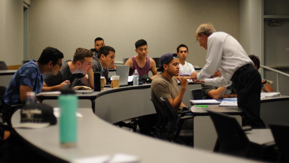
Tomorrow’s photonics experts are getting a look at the leading edge of the technology today, thanks to the AIM Photonics Research Undergraduate Apprenticeship at UC Santa Barbara. The eight-week summer research program provides community college and UCSB undergraduate students with the technical and professional training that will enable them to transition into careers in the photonics industry.
“The AIM apprentice program exposes students to leading research and gives them the opportunity to learn research skills, interact with professors and graduate students and advance state-of-the-art research,” said John Bowers, director of the UCSB-based West Coast hub of the federally funded AIM Photonics national manufacturing and research consortium. “It is a great opportunity to see if a life of research, or at least graduate school, is of interest to them.”
Bowers, an internationally renowned expert on photonics and electronics, is among a group of UCSB faculty members their graduate and postdoctoral students who have served as mentors to 11 undergraduate interns. The two-month program concludes this week with final presentations from 10 a.m. to 2:40 p.m. Tuesday, Aug. 9, at the Materials Research Lab (MRL), Room 2053, and a poster colloquium from 9:30 to 11:30 a.m. Thursday, Aug. 11, at the Corwin Pavilion. The events are free and open to the public.
As demand for telecommunications bandwidth increases — driven by the rise of mobile technology and apps, Big Data and the Internet of Things — existing telecommunications infrastructure is straining to keep up. The answer lies in photonics and optoelectronics — the use of light to transmit data with more speed, capacity and energy efficiency than conventional electronic methods. The technology is already present in the form of fiberoptic cables that transmit data over long distances.
For the true potential of photonics to be realized, however, deeper integration of the technology is required in our devices themselves (which use electrons to communicate and still require equalization to become compatible with photons), as well as in the manufacturing of the technology, where the foundries that produce fiber optics’ indium phosphide wafers are incompatible with electronics’ silicon wafers and foundries.
“In our group, the undergrad apprentices work side by side with graduate students and postdocs carrying out a portion of the research — real research, not trumped up trivial experiments whose outcome is already known,” said UCSB chemistry professor Martin Moskovits. His group studies the new physics and chemistry that arise in nanoscale systems, to investigate how size and materials composition affect optical, electrical and other properties within the infinitesimally small-scale, yet hugely important field of research.
In addition to the lectures and lab work, Moskovits’ group meets weekly with the other groups in the program, including those of chemistry and materials professor Galen Stucky and mechanical engineering professor Carl Meinhart to discuss the real-world technological problems to be solved. Interns may work in areas such as radiofrequency analog applications, photonic integrated circuit sensors and array technologies and data- and telecommunications.
Along the way, Moskovits said, interns develop working relationships and networks with others in the diverse field of photonics. They also get a taste of and assistance with the more practical aspects of a career in the sciences, from what specializations they might pursue to specific goals.
“In our case, we work closely with several groups on campus such as the Center for Science and Engineering Partnerships and the MRL, whose staff know us well and propose interns who’ve expressed interests that they know would align well with what we can offer,” he said. UCSB’s Center for Science and Engineering Partnerships is responsible for the program development, management and execution of the education and workforce development components for AIM Photonics’ West Coast hub.
The AIM Photonics undergraduate research program is part of a nationwide effort spearheaded by the Obama administration to boost tech manufacturing in the U.S., which has weakened recently due to outsourcing overseas. AIM Photonics is one of several national manufacturing consortia in a national network charged with conducting research and developing innovations in several emerging technologies, including additive manufacturing (3D printing), digital manufacturing, lightweight metal manufacturing, large-scale energy efficiency (wide bandgap semiconductors), advanced composites, flexible hybrid electronics, functional fabrics and clean energy. Alongside research and innovation, workforce development — including internships and partnerships with local industry — is required to build ample skill and opportunities for high-paying jobs in the country.
Share this article


