Sensing Potential
The science of nanomaterials and devices has advanced rapidly in the last couple of decades. Think atomically flat graphene crystals, which could have important functions in electronics or new superconductors, which could lead to low-cost medical imaging.
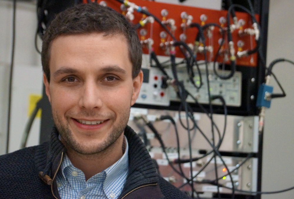
UC Santa Barbara physicist Andrea Young is ready to further advance the field of developing and characterizing nanostructured materials, thanks to a grant from the Air Force Office of Scientific Research (AFOSR) Young Investigator Research Program.
“I’m elated to have been chosen by the Air Force for this prestigious award,” said Young, an assistant professor in the Department of Physics since March 2015. “It’s really going to let us hit the ground running at UCSB.”
According to Young, much of the heavy lifting in developing advanced materials and devices revolves around the test phase — often trying to figure out why things don’t function, or behave in unexpected ways. Frequently, he added, the answer lies in the nanoscale, where imperfections and impurities in a material or device can reduce performance or lead to unanticipated phenomenologies. Taking conventional global measurements of materials — electrical resistance, for instance — goes only so far in identifying the fundamental physics, because it doesn’t dig deep enough to determine their structural cause.
“Physics of materials is complicated; when you have strongly interacting electrons and disorder, it’s very hard to calculate what is going to happen from first principles,” said Young. “So the more experimental observables you can bring to bear on a material, the more likely you are to get the right answer for what’s going on.”
Enter “nano-SQUID-on-tip,” (nSOT) a device being developed by Young and his team that aims to take simultaneous measurements of the thermal, magnetic and topographic properties of materials.
“It’s a microscope, but not the kind where you look through a lens,” he said. Essentially, it’s a sensor at the tip of tiny tube, honed to a diameter of about 50 nanometers, and brought very close to the surface of a material.
“The tip is sensitive to magnetic field and temperature,” Young said. “And if you shake it and measure how much it shakes you should be able to tell when you touch a surface, giving a view of the topography.” By combining these capabilities into a single probe, one can use the nSOT to correlate physical and magnetic structure, for example, or the spatial relationship between current flow (which produces a magnetic field) and thermal dissipation — critical for the performance of nanoscale devices. “Having a tool where you can image all these observables on the relevant length scales allows you to know quickly whether you made a material with the properties you were going for,” he said. “The real heart of this proposal is instrumentation development.”
The nSOT was first developed at the Weizmann Institute, in Israel, where Young spent time as a visiting scientist. “I’m hoping we can take the technique to the next level so it can be used on irregular materials and under more extreme conditions of temperature and magnetic field,” he said.
According to Young, this type of basic research would have broad applications in a world where new materials are continuously being developed and utilized. It could close the feedback loop between material device and device design, and characterization.
“We’re particularly interested in applying the nSOT to exotic types of low-dimension electronic states in graphene, where electrons can flow without dissipation in certain parts of the material and then only dissipate their energy at the boundary,” said Young. “But that is only one of many, many uses such a general tool will have.”
Share this article
Related Stories


