UCSB to Break Ground Friday for Building to House Pioneering California Nanosystems Institute
UC Santa Barbara will break ground this Friday, Oct. 24, for a new building to house one of the most exciting scientific endeavors the campus is currently involved in---the California NanoSystems Institute (CNSI). A special ceremony to mark the occasion will begin at 1:30 p.m. and include remarks by Congresswoman Lois Capps, California State Assemblymember Hannah-Beth Jackson, local industrial partners, UCSB Chancellor Henry T. Yang and other UC and UCLA officials.
A multidisciplinary partnership between UCLA and UC Santa Barbara, the CNSI is one of the four California Institutes for Science and Innovation established in December 2000 by Governor Gray Davis with the support of the state legislature and California industry. Corporate partners are providing $200 million in matching grants to each of the institutes, which received $100 million in state funds. While the scientific work of the CNSI is well under way in laboratories on the UCSB and UCLA campuses, the new building will serve as the hub of nanosystems research at UCSB. A CNSI building on the UCLA campus is also under construction.
By exploring the power and potential of manipulating structures molecule-by-molecule, the CNSI is on its way to creating revolutionary new materials, devices, and systems that will enhance virtually every aspect of our lives---helping to drive California's economy through innovations in medical delivery and health care, powerful new information technologies, energy efficient devices, environmental improvements, and more.
"The ability to engineer and control materials at the nanometer scale gives us the opportunity to create entirely new materials with properties that would uniquely suit them for specific applications," says Evelyn Hu, a UCSB professor of electrical and computer engineering and of materials who is co-director of the CNSI. "As nature does, we can optimize the operation and performance of the system by engineering the performance of the nanostructure components, making materials that are more optically efficient, more environmentally friendly, or more durable."
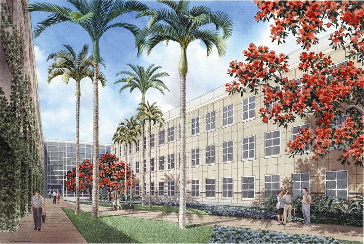
The new CNSI building will form the entryway to the eastern part of the UCSB campus. Designed to facilitate interactions among researchers from a broad range of science and engineering disciplines, these state-of-the-art facilities will bring together innovators from California universities, industries, and national laboratories.
ABOUT THE CNSI BUILDING
The CNSI building (110,904 gross square feet) will provide 61,994 assignable square feet of interdisciplinary modular research laboratories and specialized and shared laboratories for sophisticated imaging, spectroscopy, and bio-nanofabrication; digital media research laboratories; and conference and multipurpose facilities, offices, administrative space and support facilities. Collectively, these laboratories, including a state-of-the-art clean room, represent the hub of the institute's cross-disciplinary and collaborative research program.
Similarly, modular laboratories will accommodate a variety of interdisciplinary research and are designed for ease of reconfiguration to accommodate future changes in research.
Digital media research will include a sphere to provide a fully immersive 360 degree virtual visual and audio environment.
The main body of the CNSI is designed as a simple 3-story rectangular building to provide the degree of flexibility and dimensional regularity that the numerous labs, offices and conference spaces require.
In contrast, the north part of CNSI, housing multipurpose facilities and the digital lab, has been designed with an irregular geometry reflecting unique space requirements.
The Mesa Road façade of the CNSI will be distinguished by alternating vertical bands of windows and colored limestone that will impart a sense of rhythm and movement to passersby and culminate in an iconographic mural that artistically reflects the research, artistry and dynamism of the institute's research.
Located on the northeastern edge of campus south of Mesa Road, the project will integrate its landscape with the design of a proposed new East Gate entry to UCSB.
The building will cost $53 million, not including equipment and furnishings. Altoon + Porter Architects of Los Angeles are Executive Architect for this project, in association with Design Architect, Venturi, Scott Brown and Associates, Inc. of Philadelphia.
The project is being managed by the UCSB Office of Design & Construction.
Construction begins in November 2003 and is to be completed in January 2006.
ABOUT NANOSYSTEMS RESEARCH
Scientists worldwide are on the brink of a new revolution at the nanoscale, with breakthroughs occurring at the atomic level---breakthroughs that will stimulate the creation of new businesses and jobs for California.
The California NanoSystems Institute is exploring the power and potential of manipulating structures atom-by-atom to engineer new materials, devices and systems that will dramatically change virtually every aspect of our
technology.
Nanosystems is science done at the scale of a nanometer---one billionth of a meter.
The DNA molecule is two nanometers wide---roughly 1,000 times smaller than a blood cell or 10,000 times smaller than the diameter of a human hair.
Researchers are discovering ways to combine biological and engineered components to create materials and devices with unique combinations of properties.
Possible nanosystems applications include smaller, faster and more efficient computers; medicines that target the molecular errors that cause disease while leaving healthy cells unharmed; lighter, stronger, more durable building materials that may make cars, buses, planes and other forms of transportation safer and more energy efficient; a lamp that uses one-tenth as much energy as modern light bulbs and never burns out; and new products and materials created with a molecular-level precision that have characteristics well beyond what can be manufactured today.
Examples of nanosystems research under way at UCSB through the CNSI include:
Nitride Nanostructures: More Than New Light for the World
Say "semiconductor," and most people think of silicon, the material of computer chips and hence "Silicon Valley."
Gallium nitride is a compound semiconductor used to make white light emitting diodes (LEDs).
It is all but certain that white LEDs will replace the incandescent light bulb Thomas Edison invented 100 years ago.
White LEDs use much less energy than incandescent lighting.
A white LED flashlight (already commercially available) lasts five to six times longer than its incandescent-bulb counterpart.
The inventor of the white LED, UCSB's Shuji Nakamura, is a CNSI scientist.
Lumileds in San Jose and Cree in Goleta are already commercializing this technology.
The Center for Solid State Lighting and Displays at UCSB, which Nakamura directs, is now engaged in efforts to make gallium nitride in a form suitable for the mass production required to replace incandescent lighting worldwide.
Nakamura is also the inventor of the blue LED and the green LED.
The latter is most noticeable to Californians as newly installed green signal lights at road intersections.
By upgrading to 210,000 LED traffic signals (all colors, including the Nakamura green), California is saving an estimated 81,571,000 KWH per year; that energy savings translates into an annual dollars savings of $10,600,000.
Nakamura is at the center of a group of CNSI researchers who are the international leaders in the development of transformative gallium nitride technologies.
UCSB engineer Umesh Mishra leads efforts to make transistors out of gallium nitride; his team---the first to make a bipolar transistor out of gallium nitride---is closing in on crafting a field effect transistor (FET) that would replace the gallium arsenide FETs in, for instance, cell phones.
In a May 2002 cover article in "IEEE Spectrum," on "The Toughest Transistor Yet," Mishra predicts that gallium nitride will do for wireless transmission what it has done for optoelectronics:
"bring about a revolution."
Spintronics and Quantum Computing
CNSI researchers participating in the Center for Spintronics and Quantum Computation, directed by UCSB physicist David Awschalom, have seized the lead internationally in discoveries aimed at understanding and controlling electron spin in semiconducting materials.
Their research has been featured on the covers of "Science" Magazine, "Scientific American," "IEEE Spectrum," and "Discover."
Just like the charge currents that flow in ordinary "electronics," spin currents may form the foundation for a new type of "spintronics" that researchers hope will improve speed in devices for information processing including hard disk drives and nonvolatile RAM.
Particle spin is also the basis for quantum-computing paradigms.
The binary bit of conventional computing---either 0 or 1---corresponds in the spin quantum-computing paradigm to a quantum bit consisting of a particle spin that is either up or down.
What is different and what makes quantum computation a potentially richer computational approach is that the electron spin can be in a superposition of spin up and spin down. Therefore, a quantum bit can encode not just one piece of information (for instance whether a light is on or off), but much more, like the light's color or intensity.
Awschalom and collaborators have discovered how to control electron spin electrically. Most researchers approaching the spin-based paradigm for spintronics and quantum computing technologies have assumed that the behavior of spins must be controlled by magnetic fields.
The prospect of independently controlling 100 million magnets comprising a "spintronic" circuit has boggled the imagination of researchers.
By contrast, controlling 100 million devices with electrical gates is what we already do in computers sitting on a multitude of desks throughout the world.
Nanophotonics: The California Connection
Photons are particles of light, and "photonics" means using light to transport information through optical fiber (essentially glass) and manipulation of light using photonic circuits.
Optical fiber markedly outperforms other transmission media such as air, coaxial cable, or microwave tubing in terms of the bits per second that can be carried (high bandwidth) and the resulting diminution of signal per meter of travel.
The CNSI, along with the other
California Institutes for Science and Innovation (CISIs), is collaborating with CENIC, a not-for-profit entity created by major California universities to develop and deploy advanced networking services throughout the state. As an integral part of this collaboration, and to leverage the abundance of excess fiber capacity, a new network is being built in Southern California. This experimental all-glass network is a laboratory facility that puts into place a transition pipeline to enable CNSI researchers such as UCSB scientists Dan Blumenthal and Evelyn Hu to test state-of-the art, advanced optical networking and nanophotonics concepts.
This Southern California collaborative effort is linked to a larger national effort called the "National LightRail," whose mission is to enable leading-edge research in optical networking and related Internet Technologies.
CNSI and other CISIs working together with CENIC represent a huge success story for the state.
This collaborative effort gives the state a national leadership role in the development of future networking technologies and capabilities.
No other state has the critical mass of technologies that will surely come together to form new companies and jobs.
CNSI researchers ultimately aim at developing new foundations to enable integration of optical, electrical, and microelectromechanical systems (MEMS) to support the systems approach to the telecommunications technology of the future. Currently, on the information superhighway, every e-mail message turns into a plethora of "packets," which are routed electronically over different pathways before being reassembled using Internet Protocol (IP) for final delivery.
Blumenthal's research, backed by Cisco Systems, seeks to do the routing optically---to imbue, in effect, the optics with intelligence.
The integration of photonics to the level of electronics is key to the future success of optical technologies and future California companies that will lead the way in this market segment.
CNSI nanophotonics researchers are engaged in building the equivalent of an electronic circuit with light.
They have already made simple nanophotonic circuits, and are at a stage analogous to that of electronic-circuit pioneers in the 1950s and 1960s.
The key concept for technological innovation is that nanophotonic circuits can take over the job of handling the massive amounts of information coming down the optical fiber where electronic circuits have great difficulty keeping up.
CNID Channels Discovery to Defense Contractors
The Center for Nanoscale Innovation for Defense (CNID) has been created in conjunction with CNSI to facilitate the rapid transition of research innovation in the nanosciences into applications for the defense sector. Participants, in addition to CNSI, include UC Riverside, two federal agencies (Defense Agency Research Project Administration [DARPA] and Defense MicroElectronics Activity [DMEA]), the National Labs (particularly Los Alamos), and 10 industrial partners (Boeing, DuPont, Hewlett Packard, Hughes Research Laboratories, Motorola, NanoSys, Northrop Grumman, Rockwell Scientific, Raytheon, and TRW).
###
Illustrations of the planned building in electronic form are available and can be downloaded from the UCSB web site, www.ucsb.edu
For more information about Altoon + Porter and the building's design, contact Connie Hall at Christine Anderson Associates, 323 936-1447.
More information about the California NanoSystems Institute is available at the CNSI web site: www.cnsi-uc.org/
More information about CNSI at UCSB is available at www.cnsi.ucsb.edu
For more information about CNSI research at UCSB, contact Jacquelyn Savani, Director of Media Relations, CNSI, (805) 893-4301, jsavani@engineering.ucsb.edu
Related Links
Share this article
Related Stories


