The Next Wonder Semiconductor

In a study that confirms its promise as the next-generation semiconductor material, UC Santa Barbara researchers have directly visualized the photocarrier transport properties of cubic boron arsenide single crystals.
“We were able to visualize how the charge moves in our sample,” said Bolin Liao, an assistant professor of mechanical engineering in the College of Engineering. Using the only scanning ultrafast electron microscopy (SUEM) setup in operation at a U.S. university, he and his team were able to make “movies” of the generation and transport processes of a photoexcited charge in this relatively little-studied III-V semiconductor material, which has recently been recognized as having extraordinary electrical and thermal properties. In the process, they found another, beneficial property that adds to the material’s potential as the next great semiconductor.
Their research, conducted in collaboration with physics professor Zhifeng Ren’s group at the University of Houston, who specialize in fabricating high-quality single crystals of cubic boron arsenide, appears in the journal Matter.
‘Ringing the Bell’
Boron arsenide is being eyed as a potential candidate to replace silicon, the computer world’s staple semiconductor material, due to its promising performance. For one thing, with an improved charge mobility over silicon, it easily conducts current (electrons and their positively charged counterpart, “holes”). However, unlike silicon, it also conducts heat with ease.
“This material actually has 10 times higher thermal conductivity than silicon,” Liao said. This heat conducting — and releasing — ability is particularly important as electronic components become smaller and more densely packed, and pooled heat threatens the devices’ performance, he explained.
“As your cellphones become more powerful, you want to be able to dissipate the heat, otherwise you have efficiency and safety issues,” he said. “Thermal management has been a challenge for a lot of microelectronic devices.”
What gives rise to the high thermal conductivity of this material, it turns out, can also lead to interesting transport properties of photocarriers, which are the charges excited by light, for example, in a solar cell. If experimentally verified, this would indicate that cubic boron arsenide can also be a promising material for photovoltaic and light detection applications. Direct measurement of photocarrier transport in cubic boron arsenide, however, has been challenging due to the small size of available high-quality samples.
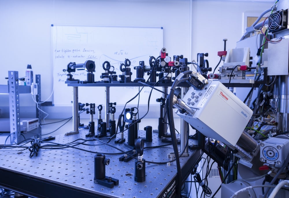
The research team’s study combines two feats: The crystal growth skills of the University of Houston team, and the imaging prowess at UC Santa Barbara. Combining the abilities of the scanning electron microscope and femtosecond ultrafast lasers, the UCSB team built what is essentially an extremely fast, exceptionally high-resolution camera.
“Electron microscopes have very good spatial resolution — they can resolve single atoms with their sub-nanometer spatial resolution — but they’re typically very slow,” Liao said, noting this makes them excellent for capturing static images.
“With our technique, we couple this very high spatial resolution with an ultrafast laser, which acts as a very fast shutter, for extremely high time resolution,” Liao continued. “We’re talking about one picosecond — a millionth of a millionth of a second. So we can make movies of these microscopic energy and charge transport processes.” Originally invented at Caltech, the method was further developed and improved at UCSB from scratch and now is the only operational SUEM setup at an American university.
“What happens is that we have one pulse of this laser that excites the sample,” explained graduate student researcher Usama Choudhry, the lead author of the Matter paper. “You can think of it like ringing a bell; it’s a loud noise that slowly diminishes over time.” As they “ring the bell,” he explained, a second laser pulse is focused onto a photocathode (“electron gun”) to generate a short electron pulse to image the sample. They then scan the electron pulse over time to gain a full picture of the ring. “Just by taking a lot of these scans, you can get a movie of how the electrons and holes get excited and eventually go back to normal,” he said.
Among the things they observed while exciting their sample and watching the electrons return to their original state is how long the “hot” electrons persist.
“We found, surprisingly, the ‘hot’ electrons excited by light in this material can persist for much longer times than in conventional semiconductors,” Liao said. These “hot” carriers were seen to persist for more that 200 picoseconds, a property that is related to the same feature that is responsible for the material’s high thermal conductivity. This ability to host “hot” electrons for significantly longer amounts of time has important implications.
“For example, when you excite the electrons in a typical solar cell with light, not every electron has the same amount of energy,” Choudhry explained. “The high-energy electrons have a very short lifetime, and the low-energy electrons have a very long lifetime.” When it comes to harvesting the energy from a typical solar cell, he continued, only the low-energy electrons are efficiently being collected; the high-energy ones tend to lose their energy rapidly as heat. Because of the persistence of the high-energy carriers, if this material was used as a solar cell, more energy could efficiently be harvested from it.
With boron arsenide beating silicon in three relevant areas — charge mobility, thermal conductivity and hot photocarrier transport time — it has the potential to become the electronics world’s next state-of-the-art material. However, it still faces significant hurdles — fabrication of high-quality crystals in large quantities — before it can compete with silicon, enormous amounts of which can be manufactured relatively cheaply and with high quality. But Liao doesn’t see too much of a problem.
“Silicon is now routinely available because of years of investment; people started developing silicon around the 1930s and ‘40s,” he said. “I think once people recognize the potential of this material, there will be more effort put into finding ways to grow and use it. UCSB is actually uniquely positioned for this challenge with strong expertise in semiconductor development.”
The work conducted at UCSB was partially supported by the U.S. Department of Energy, Office of Basic Energy Sciences, under the award number DE-SC0019244 for the development of SUEM, and by the U.S. Army Research Office under award number W911NF-19-1-0060 for studying photocarrier dynamics in emerging materials. The growth of boron arsenide crystals at the University of Houston was supported by the U.S. Office of Naval Research under award number N00014-16-1-2436.
Share this article
Related Stories